
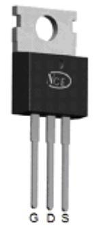
VDS =250V,ID =80A RDS(ON) <18.5mΩ @ VGS=10V
Excellent gate charge x RDS(on) product
Very low on-resistance RDS(on)
175 °C operating temperature
Pb-free lead plating
100% UIS tested
VDS=250V,ID=80A RDS(ON)<18.5mΩ @ VGS=10V
Excellent gate charge x RDS(on) product
Very low on-resistance RDS(on)
175 °C operating temperature
Pb-free lead plating 100% UIS tested
VDS =250V,ID =80A RDS(ON) <18.5mΩ @ VGS=10V
Excellent gate charge x RDS(on) product
Very low on-resistance RDS(on)
175 °C operating temperature
Pb-free lead plating
100% UIS tested
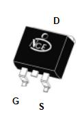
VDS =250V,ID =90A RDS(ON) <15mΩ @ VGS=10V
Excellent gate charge x RDS(on) product
Very low on-resistance RDS(on)
175 °C operating temperature
Pb-free lead plating
Optimized body diode reverse recovery performance
VDS =250V,ID =90A RDS(ON) <15mΩ @ VGS=10V
Excellent gate charge x RDS(on) product
Very low on-resistance RDS(on)
175 °C operating temperature
Pb-free lead plating
Optimized body diode reverse recovery performance
VDS =250V,ID =90A RDS(ON) <15mΩ @ VGS=10V
Excellent gate charge x RDS(on) product
Very low on-resistance RDS(on)
175 °C operating temperature
Pb-free lead plating
Optimized body diode reverse recovery performance
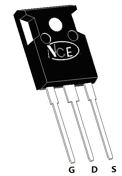
VDS=250V,ID=90ARDS(ON)<16mΩ @ VGS=10V
Excellent gate charge x RDS(on)product
Very low on-resistance RDS(on)
175 °C operating temperature
Pb-free lead plating
Optimized body diode reverse recovery performance
