
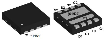
Q1 "High Side" MOSFET:VDS =30V,ID =20A;RDS(ON) <8.5mΩ @ VGS=10V;RDS(ON)<14mΩ @ VGS=4.5V
Q2 "Low Side" MOSFET:VDS =30V,ID =35A;RDS(ON) <7mΩ @ VGS=10V;RDS(ON) <12mΩ @ VGS=4.5V
Excellent gate charge x RDS(on) product(FOM)
Very low on-resistance RDS(on)
150 °C operating temperature
Pb-free lead plating
100% UIS tested
Q1 "High Side" MOSFET:VDS =30V,ID =15A;RDS(ON) <11.5mΩ @ VGS=10V;RDS(ON)<19mΩ @ VGS=4.5V
Q2 "Low Side" MOSFET:VDS =30V,ID =20A;RDS(ON) <8.2mΩ @ VGS=10V;RDS(ON) <13mΩ @ VGS=4.5V
Excellent gate charge x RDS(on) product(FOM)
Very low on-resistance RDS(on)
150 °C operating temperature
Pb-free lead plating
100% UIS tested
DC/DC Converter
Ideal for high-frequency switching and synchronous rectification
DC/DC Converter
Ideal for high-frequency switching and synchronous rectification
